(Hong Kong)

Product Summary
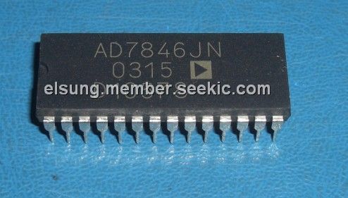
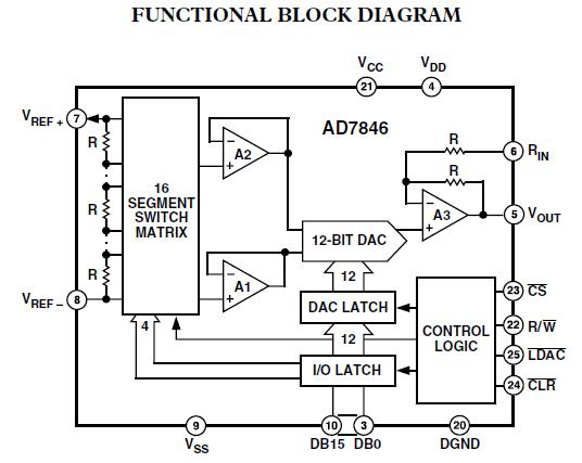
The AD7846JN is a 16-bit DAC constructed with LC2MOS process. The AD7846JN has VREF+ and VREF– reference inputs and an on-chip output amplifier. These can be configured to give a unipolar output range (0 V to +5 V, 0 V to +10 V) or bipolar output ranges (±5 V, ±10 V). The AD7846JN uses a segmented architecture. The 4 MSBs in the AD7846JN latch select one of the segments in a 16-resistor string. Both taps of the segment are buffered by amplifiers and fed to a 12-bit DAC, which provides a further 12 bits of resolution. This architecture ensures 16-bit monotonicity. Excellent integral linearity results from tight matching between the input offset voltages of the two buffer amplifiers.
Parametrics
AD7846JN absolute maximum ratings: (1)VDD to DGND: –0.4 V to +17 V; (2)VCC to DGND: –0.4 V, VDD + 0.4 V or +7 V; (3)VSS to DGND: +0.4 V to –17 V; (4)VREF+ to DGND: VDD + 0.4 V, VSS – 0.4 V; (5)VREF– to DGND: VDD + 0.4 V, VSS – 0.4 V; (6)VOUT to DGND2: VDD + 0.4 V, VSS – 0.4 V or ±10 V; (7)RIN to DGND: VDD + 0.4 V, VSS – 0.4 V; (8)Digital Input Voltage to DGND: –0.4 V to VCC + 0.4 V; (9)Digital Output Voltage to DGND: –0.4 V to VCC + 0.4 V; (10)Power Dissipation (Any Package) To +75℃: 1000 mW; Derates above +75℃: 10 mW/℃; (11)Operating Temperature Range: 0 to +70℃; (12)Storage Temperature Range: –65 to +150℃; (13)Lead Temperature (Soldering): +300℃.
Features
AD7846JN features: (1)16-Bit Monotonicity over Temperature; (2)±2 LSBs Integral Linearity Error; (3)Microprocessor Compatible with Readback Capability; (4)Unipolar or Bipolar Output; (5)Multiplying Capability; (6)Low Power (100 mW Typical).
Diagrams
| Image | Part No | Mfg | Description |  |
Pricing (USD) |
Quantity | ||||||||||||||
|---|---|---|---|---|---|---|---|---|---|---|---|---|---|---|---|---|---|---|---|---|
 |
 AD7846JN |
|
IC DAC 16BIT LC2MOS VOUT 28-DIP |
Data Sheet |
|
|
||||||||||||||
|
AD7846JNZ |
|
IC DAC 16BIT LC2MOS VOUT 28-DIP |
Data Sheet |
|
|
||||||||||||||